

Sell Your Semiconductor Tooling Business — CHIPS Act M&A Advisory for Equipment & Component Suppliers
You have spent decades mastering the nanometer tolerances and cleanroom protocols required to keep the global fabs running. When it comes time to exit, you need an advisor who understands that your value isn't just in your equipment—it's in your spec-in status with Tier 1 OEMs and your mastery of advanced materials.
The 2026 M&A Landscape for Semiconductor Tooling
The "CHIPS Act" era has fundamentally shifted how semiconductor supply chain businesses are valued. Generalist brokers often fail to quantify the "Technical Moat" of a business, looking only at historical EBITDA without accounting for the massive CAPEX requirements or the scarcity of specialized labor. At The Precision Firm, we speak the language of the cleanroom and the boardroom, ensuring your proprietary processes are monetized at their true market value.
Intellectual Property & "Spec-In" Status: Buyers are paying a heavy premium for firms that are "designed-in" to the next generation of lithography or deposition tools, creating high switching costs for OEMs.
Material Science Mastery: Expertise in machining Silicon Carbide (SiC), Gallium Nitride (GaN), or ultra-high-purity plastics like PEEK provides a significant competitive advantage over standard metal shops.
Cleanroom Infrastructure: Existing ISO Class 5 or Class 6 cleanroom facilities represent a massive "avoided cost" for buyers, allowing for immediate production scaling without the 18-month lead time for new construction.
Technical Competencies We Represent in Semiconductor Tooling
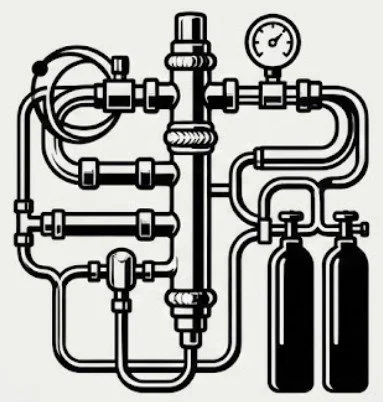
High-Purity Fluid Handling & Gas Delivery
Focus Area: The fabrication of ultra-high purity (UHP) gas panels, orbital welding, and chemical delivery systems used in wafer processing.
Icon Suggestion: A schematic of a manifold with orbital weld beads.
Equipment & Labor: Orbital welders (AMI), Helium leak detectors, and certified Class 100 cleanroom technicians.
The Buyer Pool: Strategic HVAC/Fluid control giants or Private Equity firms building a "front-end" wafer fab service platform.
Key Certification: SEMI S2 Safety Standards and ISO 9001:2015.

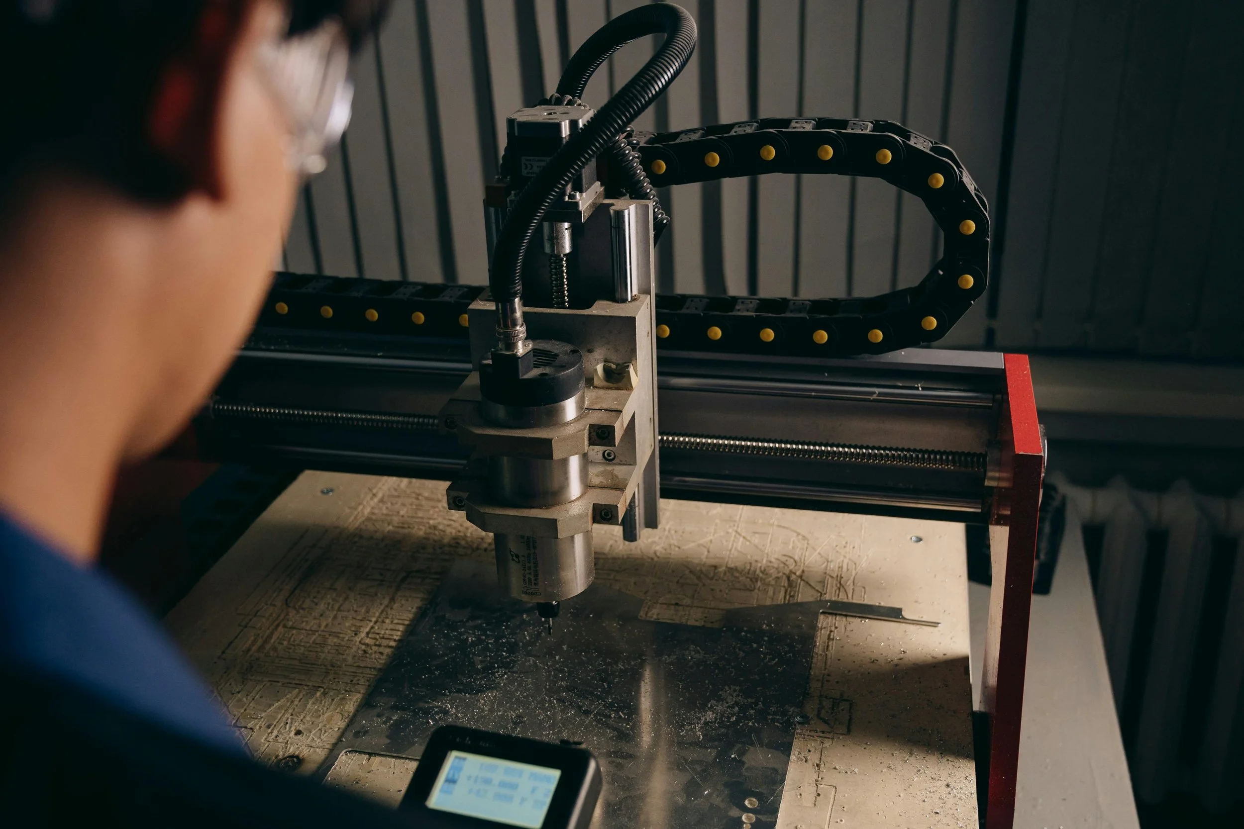
Precision Machining of Advanced Materials
Focus Area: Sub-micron tolerance machining of ceramic, quartz, and refractory metals for ion implantation and etching tools.
Icon Suggestion: A 5-axis CNC spindle head milling a complex ceramic part.
Equipment & Labor: 5-axis Mazak or Hermle centers, Wire EDM (Sodik/Fanuc), and "Red-Badge" machinists capable of working with exotic alloys.
The Buyer Pool: Larger Tier 1 aerospace/defense contractors looking to diversify into the semiconductor "moat."
Key Certification: AS9100D (frequently required for dual-use technologies) or Nadcap.
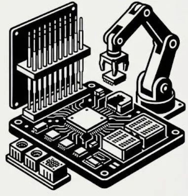
Automated Test Equipment (ATE) & Back-End Tooling
Focus Area: Engineering and assembly of test sockets, probe cards, and burn-in boards for the assembly and test (OSAT) phase.
Icon Suggestion: A high-density probe card array.
Equipment & Labor: High-speed SMT lines, automated optical inspection (AOI), and electrical engineers specializing in signal integrity.
The Buyer Pool: Global OSAT providers or specialized electronics manufacturing services (EMS) firms.
Key Certification: ISO 13485 (if dual-tracked for medical) or ESD S20.20.

Navigating Industry-Specific Compliance in M&A
ITAR and EAR Export Controls
The Problem: Many semiconductor tools fall under "Dual-Use" categories, meaning a sale to a foreign-backed buyer can trigger CFIUS (Committee on Foreign Investment in the United States) reviews, potentially killing a deal or delaying it by years.
The Solution: The Precision Firm conducts a "pre-market" export control audit to identify controlled technical data, ensuring we only target buyers who can clear the regulatory hurdles of the Directorate of Defense Trade Controls (DDTC).
Tier 1 Supplier Re-Certification Risk
The Problem: A change in ownership often triggers a mandatory "Quality Audit" from major customers like ASML, Applied Materials, or Lam Research, which can threaten the stability of the contract backlog.
The Solution: We structure deals with "Transition Services Agreements" (TSAs) that keep key quality managers in place through the re-certification window, de-risking the transition for the buyer and protecting the purchase price.
Environmental & SEMI S2 Compliance
The Problem: Legacy facilities may have "Environmental Debt" related to chemical handling or non-compliant safety protocols that can lead to massive holdbacks in escrow during a sale.
The Solution: We perform a gap analysis against current SEMI S2/S8 standards prior to listing, allowing you to remediate safety or environmental issues and present a "turnkey" compliant facility to the market.
How We Value a Semiconductor Tooling Business
We represented a semiconductor component machining shop — ISO Class 6 cleanroom, 'spec-in' status with two Tier 1 lithography OEMs, $3.4M EBITDA — at a time when a generalist had valued them at 4.5x based on equipment book value. We built the CIM around their CHIPS Act tailwinds, their cleanroom avoided-cost advantage ($8M+ to replicate), and their next-gen wafer processing program positions. Closed at 10x with a strategic OEM looking to on-shore critical supply capacity.
At The Precision Firm, we speak the language of the cleanroom and the boardroom. Your 'spec-in' status, your cleanroom infrastructure, and your mastery of advanced materials like SiC and GaN are the moats that drive the highest EBITDA multiples in the precision manufacturing sector.
Barrier to Entry (CAPEX Replacement Cost): The cost to build a modern, cleanroom-equipped, 5-axis facility is at an all-time high. Buyers will pay a premium to acquire an existing, operational footprint rather than facing the 24-month lead times for new equipment and facility build-outs.
Recurring Contract Revenue & Backlog: Unlike general job shops that bid on every project, semiconductor tooling firms often have "LTSAs" (Long Term Service Agreements) that provide predictable, high-margin revenue, which commands a higher valuation multiple.
The Talent Moat: The scarcity of engineers and machinists who understand the "Semi-Spec" is a major driver of M&A activity. In many cases, you are being valued for your "Human Capital" and the proprietary tribal knowledge required to maintain wafer yields.
Request a free confidential valuation today.
Frequently Asked Questions: Selling a Semiconductor Tooling Business
-
A: Semiconductor tooling businesses command a "Technical Premium," typically trading at 2-3 turns higher on EBITDA multiples than general job shops due to extreme barriers to entry and mission-critical integration into the global chip supply chain. While a general shop might trade at 4x-6x EBITDA, a specialized semiconductor supplier with "spec-in" status can often see 7x-10x+.
-
A: SEMI S2 and S8 certifications act as a mandatory value-gate; shops with documented compliance for environmental, health, and safety standards are viewed as "de-risked" assets. Without these, buyers will often apply a discount to the valuation to account for the cost and risk of bringing the facility up to Tier 1 standards.
-
A: Contract Backlog is treated as a primary indicator of future revenue stability and is often used to justify a "forward-looking" multiple. We work to prove the "stickiness" of this backlog by demonstrating your historical win rate and the specific "Program Life" of the tools you support.
-
A: Customer relationships are protected through a "Blind Teaser" approach and phased disclosure, ensuring your name and specific contracts are not revealed until a qualified buyer has signed a binding NDA and shown proof of funds. We manage the flow of information to ensure your customers and employees only learn of the sale at the optimal time.
-
A: A typical industrial M&A exit in the semiconductor space takes 6 to 9 months. This includes 1-2 months of preparation and valuation, 2-3 months of marketing and LOI negotiations, and 60-90 days for technical due diligence and closing.
-
A: Semiconductor tooling companies are valued on EBITDA multiples ranging from 5x to 10x+ depending on spec-in status with Tier 1 OEM customers (ASML, Applied Materials, Lam Research), cleanroom infrastructure, and material science specialization (SiC, GaN, PEEK). CHIPS Act domestic sourcing premiums are actively expanding multiples in this vertical.
-
A: Three primary drivers: (1) Spec-in status — if a buyer's competitor would need 18+ months to replicate your OEM design-ins, that's a hard moat. (2) Cleanroom infrastructure — ISO Class 5/6 facilities represent -5M+ in avoided build cost. (3) Materials expertise — SiC, GaN, and ultra-high-purity plastics are scarce skills driving scarcity premiums.
-
A: Strategic acquirers include SEMI equipment OEMs (ASML, Applied Materials, LAM) seeking to vertically integrate domestic supply. Financial buyers include PE groups building CHIPS Act-adjacent platforms. Cross-sector buyers from aerospace/defense see semiconductor as a natural adjacency due to shared materials expertise.
Related Resources
Ready to Maximize the Value of Your Semiconductor Tooling Business?
At The Precision Firm, we aren't just "bankers"—we are former operators and engineers who have spent time on the shop floor. We understand the difference between a standard CNC mill and a high-speed machining center dedicated to Silicon Carbide. We know what a "Tier 1" audit looks like, and we know how to position your technical expertise to command a premium in the market.
Don't leave your legacy to a generalist. Let's discuss your technical enterprise value today.